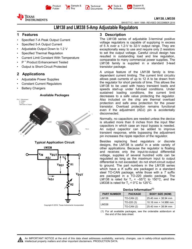
Product Folder Sample & Buy Technical Documents Support & Community Tools & Software LM138, LM338 SNVS771C – MAY 1998 – REVISED DECEMBER 2016 LM138 and LM338 5-Amp Adjustable Regulators 1 Features 3 Description • • • • • • • The LM138 series of adjustable 3-terminal positive voltage regulators is capable of supplying in excess of 5 A over a 1.2-V to 32-V output range. They are exceptionally easy to use and require only 2 resistors to set the output voltage. Careful circuit design has resulted in outstanding load and line regulation, comparable to many commercial power supplies. The LM138 family is supplied in a standard 3-lead transistor package. Specified 7-A Peak Output Current Specified 5-A Output Current Adjustable Output Down to 1.2 V Specified Thermal Regulation Current Limit Constant With Temperature P + Product Enhancement Tested Output is Short-Circuit Protected 1 2 Applications • • • Adjustable Power Supplies Constant Current Regulators Battery Chargers Available Packages Pin 1. Adjustment 2. Output 3. Input Tab/Case is Output 3 1 TO-220 TO-3 1 2 3 Typical Application Circuit A unique feature of the LM138 family is timedependent current limiting. The current limit circuitry allows peak currents of up to 12 A to be drawn from the regulator for short periods of time. This allows the LM138 to be used with heavy transient loads and speeds start-up under full-load conditions. Under sustained loading conditions, the current limit decreases to a safe value protecting the regulator. Also included on the chip are thermal overload protection and safe area protection for the power transistor. Overload protection remains functional even if the adjustment (ADJ) pin is accidentally disconnected. Normally, no capacitors are needed unless the device is situated more than 6 inches from the input filter capacitors in which case an input bypass is needed. An output capacitor can be added to improve transient response, while bypassing the adjustment pin increases the ripple rejection of the regulator. Besides replacing fixed regulators or discrete designs, the LM138 is useful in a wide variety of other applications. Because the regulator is floating and receives only the input-to-output differential voltage, supplies of several hundred volts can be regulated as long as the maximum input to output differential is not exceeded; do not short-circuit output to ground. The part numbers in the LM138 series which have a K suffix are packaged in a standard steel TO-CAN package, while those with a T suffix are packaged in a TO-220 plastic package. The LM138 is rated for TJ = –55°C to 150°C, and the LM338 is rated for TJ = 0°C to 125°C. Device Information(1) PART NUMBER LM138 Copyright © 2016, Texas Instruments Incorporated LM338 PACKAGE BODY SIZE (NOM) TO-CAN (2) 25.40 mm × 38.94 mm TO-220 (3) 10.16 mm × 14.986 mm TO-CAN (2) 25.40 mm × 38.94 mm (1) For all available packages, see the orderable addendum at the end of the data sheet. 1 An IMPORTANT NOTICE at the end of this data sheet addresses availability, warranty, changes, use in safety-critical applications, intellectual property matters and other important disclaimers. PRODUCTION DATA. LM138, LM338 SNVS771C – MAY 1998 – REVISED DECEMBER 2016 www.ti.com Table of Contents 1 2 3 4 5 6 7 Features .................................................................. Applications ........................................................... Description ............................................................. Revision History..................................................... Pin Configuration and Functions ......................... Specifications......................................................... 1 1 1 2 3 3 6.1 6.2 6.3 6.4 6.5 6.6 3 3 4 4 5 6 Absolute Maximum Ratings ...................................... Recommended Operating Conditions....................... Thermal Information .................................................. Electrical Characteristics: LM138.............................. Electrical Characteristics: LM338.............................. Typical Characteristics .............................................. Detailed Description .............................................. 9 7.1 7.2 7.3 7.4 Overview ................................................................... 9 Functional Block Diagram ......................................... 9 Feature Description................................................... 9 Device Functional Modes........................................ 10 8 Application and Implementation ........................ 11 8.1 Application Information............................................ 11 8.2 Typical Applications ................................................ 12 8.3 System Examples ................................................... 17 9 Power Supply Recommendations...................... 23 10 Layout................................................................... 23 10.1 Layout Guidelines ................................................. 23 10.2 Layout Example .................................................... 23 11 Device and Documentation Support ................. 24 11.1 11.2 11.3 11.4 11.5 11.6 Receiving Notification of Documentation Updates Related Links ........................................................ Community Resources.......................................... Trademarks ........................................................... Electrostatic Discharge Caution ............................ Glossary ................................................................ 24 24 24 24 24 24 12 Mechanical, Packaging, and Orderable Information ........................................................... 24 4 Revision History NOTE: Page numbers for previous revisions may differ from page numbers in the current version. Changes from Revision B (April 2013) to Revision C Page • Added Device Information table, Pin Configuration and Functions section, Specifications section, Recommended Operating Conditions table, Thermal Information table, Detailed Description section, Application and Implementation section, Power Supply Recommendations section, Layout section, Device and Documentation Support section, and Mechanical, Packaging, and Orderable Information section .................................................................................................. 1 • Deleted RETS138K military specification reference from Absolute Maximum Ratings table................................................. 3 • Changed Junction to Ambient, RθJA, value in Thermal Information table From: 50°C/W To: 22.9°C/W (NDE) ..................... 4 • Changed Junction to Case, RθJC(top), value in Thermal Information table From: 4°C/W To: 15.7°C/W (NDE) ....................... 4 Changes from Revision A (April 2013) to Revision B • 2 Page Changed layout of National Semiconductor Data Sheet to TI format .................................................................................... 1 Submit Documentation Feedback Copyright © 1998–2016, Texas Instruments Incorporated Product Folder Links: LM138 LM338 LM138, LM338 www.ti.com SNVS771C – MAY 1998 – REVISED DECEMBER 2016 5 Pin Configuration and Functions NDS Package 2-Pin TO-CAN Bottom View NDE Package 3-Pin TO-220 Front View Package Number NDE0003B Package Number NDS0002A Pin Functions PIN NAME TO-220 TO-CAN ADJ 1 1 VIN 3 VOUT 2 I/O DESCRIPTION I Output voltage adjustment pin. Connect to a resistor divider to set VO 2 I Supply input pin Case O Voltage output pin 6 Specifications 6.1 Absolute Maximum Ratings over operating free-air temperature range (unless otherwise noted) (1) MIN MAX UNIT Input and output voltage differential –0.3 40 V Power dissipation Internally limited Lead temperature Operating temperature, TJ TO-3 package (soldering, 10 s) 300 TO-220 package (soldering, 4 s) 260 LM138 –55 150 LM338 0 125 –65 150 Storage temperature, Tstg (1) °C °C °C Stresses beyond those listed under Absolute Maximum Ratings may cause permanent damage to the device. These are stress ratings only, which do not imply functional operation of the device at these or any other conditions beyond those indicated under Recommended Operating Conditions. Exposure to absolute-maximum-rated conditions for extended periods may affect device reliability. 6.2 Recommended Operating Conditions over operating free-air temperature range (unless otherwise noted) Input-to-output voltage differential Output current MIN MAX 3 40 UNIT V 5 A Submit Documentation Feedback Copyright © 1998–2016, Texas Instruments Incorporated Product Folder Links: LM138 LM338 3 LM138, LM338 SNVS771C – MAY 1998 – REVISED DECEMBER 2016 www.ti.com 6.3 Thermal Information LM338 THERMAL METRIC (1) LM338 NDS (TO-CAN) NDE (TO-220) NDS (TO-CAN) 2 PINS 3 PINS 2 PINS 35 22.9 35 °C/W RθJC(top) Junction-to-case (top) thermal resistance 1 15.7 1 °C/W RθJB Junction-to-board thermal resistance — 4.1 — °C/W ψJT Junction-to-top characterization parameter — 2.1 — °C/W ψJB Junction-to-board characterization parameter — 4.1 — °C/W RθJC(bot) Junction-to-case (bottom) thermal resistance — 0.7 — °C/W RθJA (1) Junction-to-ambient thermal resistance UNIT For more information about traditional and new thermal metrics, see the Semiconductor and IC Package Thermal Metrics application report. 6.4 Electrical Characteristics: LM138 Values apply for TJ = 25°C; VIN – VOUT = 5 V; and IOUT = 10 mA (unless otherwise noted). (1) PARAMETER TEST CONDITIONS VREF Reference voltage 3 V ≤ (VIN – VOUT) ≤ 35 V, 10 mA ≤ IOUT ≤ 5 A, P ≤ 50 W, TJ = –55°C to 150°C VRLINE Line regulation 3 V ≤ (VIN – VOUT) ≤ 35 V (2) MIN TYP MAX UNIT 1.19 1.24 1.29 V 0.005% 0.01% V 0.02% 0.04% V TJ = 25°C TJ = –55°C to 150°C TJ = 25°C 0.1% 0.3% 0.3% 0.6% Load regulation 10 mA ≤ IOUT ≤ 5 A (2) Thermal regulation 20 ms pulse IADJ Adjustment pin current TJ = –55°C to 150°C 45 100 µA ΔIADJ Adjustment pin current change 10 mA ≤ IOUT ≤ 5 A, 3 V ≤ (VIN – VOUT) ≤ 35 V, TJ = –55°C to 150°C 0.2 5 µA ΔVR/T Temperature stability TJ = –55°C to 150°C 1% VIN – VOUT = 35 V, TJ = –55°C to 150°C 3.5 5 mA VRLOAD ILOAD(MIN) Minimum load current TJ = –55°C to 150°C 0.002% 0.01% W VIN – VOUT ≤ 10 V ICL Current limit VN RMS output noise (percent of VOUT) ΔVR/ΔVIN Ripple rejection ratio Long-term stability (1) (2) 4 DC, TJ = –55°C to 150°C 5 8 A 0.5-ms peak, TJ = –55°C to 150°C 7 12 A VIN – VOUT = 30 V 1 10 Hz ≤ f ≤ 10 kHz 0.003% VOUT = 10 V, f = 120 Hz, CADJ = 0 µF, TJ = –55°C to 150°C VOUT = 10 V, f = 120 Hz, CADJ = 10 µF, TJ = –55°C to 150°C TJ = 125°C, 1000 Hrs 60 1 A 60 dB 75 dB 0.3% 1% These specifications are applicable for power dissipations up to 50 W for the TO-3 (NDS) package and 25 W for the TO-220 (NDE) package. Power dissipation is specified at these values up to 15-V input-output differential. Above 15-V differential, power dissipation is limited by internal protection circuitry. All limits (that is, the numbers in the minimum and maximum columns) are specified to TI's AOQL (Average Outgoing Quality Level). Regulation is measured at a constant junction temperature, using pulse testing with a low duty cycle. Changes in output voltage due to heating effects are covered under the specifications for thermal regulation. Submit Documentation Feedback Copyright © 1998–2016, Texas Instruments Incorporated Product Folder Links: LM138 LM338 LM138, LM338 www.ti.com SNVS771C – MAY 1998 – REVISED DECEMBER 2016 6.5 Electrical Characteristics: LM338 Values apply for TJ = 25°C; VIN – VOUT = 5 V; and IOUT = 10 mA (unless otherwise noted). (1) PARAMETER TEST CONDITIONS MIN TYP MAX UNIT 1.19 1.24 1.29 V 0.005% 0.03% V 0.02% 0.06% V VREF Reference voltage 3 V ≤ (VIN – VOUT) ≤ 35 V, 10 mA ≤ IOUT ≤ 5 A, P ≤ 50 W, TJ = 0°C to 125°C VRLINE Line regulation 3 V ≤ (VIN – VOUT) ≤ 35 V (2) VRLOAD Load regulation 10 mA ≤ IOUT ≤ 5 A (2) Thermal regulation 20-ms pulse Adjustment pin current TJ = 0°C to 125°C 45 100 µA ΔIADJ Adjustment pin current change 10 mA ≤ IOUT ≤ 5 A, 3 V ≤ (VIN – VOUT) ≤ 35 V, TJ = 0°C to 125°C 0.2 5 µA ΔVR/T Temperature stability TJ = 0°C to 125°C 10 mA IADJ ILOAD(MIN) Minimum load current TJ = 25°C TJ = 0°C to 125°C TJ = 25°C 0.1 0.5 TJ = 0°C to 125°C 0.3 1 0.002% 0.02% W 1 VIN – VOUT = 35 V, TJ = 0°C to 125°C 3.5 VIN – VOUT ≤ 10 V ICL Current limit DC, TJ = 0°C to 125°C 5 8 0.5-ms peak, TJ = 0°C to 125°C 7 12 VIN – VOUT = 30 V VN RMS output noise (percent of VOUT) ΔVR/ΔVIN Ripple rejection ratio Long-term stability (1) (2) A 0.003% VOUT = 10 V, f = 120 Hz, CADJ = 0 µF, TJ = 0°C to 125°C TJ = 125°C, 1000 Hrs A 1 10 Hz ≤ f ≤ 10 kHz VOUT = 10 V, f = 120 Hz, CADJ = 10 µF, TJ = 0°C to 125°C A 60 60 dB 75 dB 0.3% 1% These specifications are applicable for power dissipations up to 50 W for the TO-3 (NDS) package and 25 W for the TO-220 (NDE) package. Power dissipation is specified at these values up to 15-V input-output differential. Above 15-V differential, power dissipation is limited by internal protection circuitry. All limits (that is, the numbers in the minimum and maximum columns) are specified to TI's AOQL (Average Outgoing Quality Level). Regulation is measured at a constant junction temperature, using pulse testing with a low duty cycle. Changes in output voltage due to heating effects are covered under the specifications for thermal regulation. Submit Documentation Feedback Copyright © 1998–2016, Texas Instruments Incorporated Product Folder Links: LM138 LM338 5 LM138, LM338 SNVS771C – MAY 1998 – REVISED DECEMBER 2016 www.ti.com 6.6 Typical Characteristics Figure 1. Current Limit Figure 2. Current Limit Figure 4. Load Regulation Figure 3. Current Limit Figure 6. Adjustment Current Figure 5. Dropout Voltage 6 Submit Documentation Feedback Copyright © 1998–2016, Texas Instruments Incorporated Product Folder Links: LM138 LM338 LM138, LM338 www.ti.com SNVS771C – MAY 1998 – REVISED DECEMBER 2016 Typical Characteristics (continued) Figure 7. Temperature Stability Figure 8. Output Impedance Figure 9. Minimum Operating Current Figure 10. Ripple Rejection Figure 11. Ripple Rejection Figure 12. Ripple Rejection Submit Documentation Feedback Copyright © 1998–2016, Texas Instruments Incorporated Product Folder Links: LM138 LM338 7 LM138, LM338 SNVS771C – MAY 1998 – REVISED DECEMBER 2016 www.ti.com Typical Characteristics (continued) Figure 13. Line Transient Response 8 Submit Documentation Feedback Figure 14. Load Transient Response Copyright © 1998–2016, Texas Instruments Incorporated Product Folder Links: LM138 LM338 LM138, LM338 www.ti.com SNVS771C – MAY 1998 – REVISED DECEMBER 2016 7 Detailed Description 7.1 Overview The LM138 and LM338 devices are adjustable, three-terminal, positive-voltage regulators capable of supplying more than 5 A over an output-voltage range of 1.2 V to 32 V. It requires only two external resistors to set the output voltage. These devices feature a typical line regulation of 0.005% and typical load regulation of 0.1%. It includes time-dependent current limiting, thermal overload protection, and safe operating area protection. Overload protection remains functional even if the ADJUST terminal is disconnected. The LM138 and LM338 devices are versatile in their applications, including uses in programmable output regulation and local on-card regulation. Or, by connecting a fixed resistor between the ADJUST and OUTPUT terminals, the LM138 and LM338 devices can function as a precision current regulators. An optional output capacitor can be added to improve transient response. The ADJUST terminal can be bypassed to achieve very high ripple-rejection ratios, which are difficult to achieve with standard three-terminal regulators. 7.2 Functional Block Diagram 7.3 Feature Description 7.3.1 NPN Darlington Output Drive NPN Darlington output topology provides naturally low output impedance and an output capacitor is optional. To support maximum current and lowest temperature, 3-V headroom is recommended (VI – VO). 7.3.2 Overload Block Overcurrent and overtemperature shutdown protects the device against overload or damage from operating in excessive heat. 7.3.3 Programmable Feedback Op amp with 1.25-V offset input at the ADJUST terminal provides easy output voltage or current (not both) programming. For current regulation applications, a single resistor whose resistance value is 1.25 V/IO and power rating is greater than 1.25 V2/R must be used. For voltage regulation applications, two resistors set the output voltage. Submit Documentation Feedback Copyright © 1998–2016, Texas Instruments Incorporated Product Folder Links: LM138 LM338 9 LM138, LM338 SNVS771C – MAY 1998 – REVISED DECEMBER 2016 www.ti.com 7.4 Device Functional Modes 7.4.1 Normal Operation The device OUTPUT pin sources current necessary to make OUTPUT pin 1.25 V greater than ADJUST terminal to provide output regulation. 7.4.2 Operation With Low Input Voltage The device requires up to 3-V headroom (VI – VO) to operate in regulation. With less headroom, the device may drop out and OUTPUT voltage is INPUT voltage minus drop out voltage. 7.4.3 Operation at Light Loads The device passes its bias current to the OUTPUT pin. The load or feedback must consume this minimum current for regulation or the output may be too high. A 250-Ω feedback resistor between OUTPUT and ADJUST consumes the worst case minimum load current of 5 mA. 7.4.4 Operation in Self Protection When an overload occurs, the device shuts down Darlington NPN output stage or reduces the output current to prevent device damage. The device automatically resets from the overload. The output may be reduced or alternate between on and off until the overload is removed. 10 Submit Documentation Feedback Copyright © 1998–2016, Texas Instruments Incorporated Product Folder Links: LM138 LM338 LM138, LM338 www.ti.com SNVS771C – MAY 1998 – REVISED DECEMBER 2016 8 Application and Implementation NOTE Information in the following applications sections is not part of the TI component specification, and TI does not warrant its accuracy or completeness. TI’s customers are responsible for determining suitability of components for their purposes. Customers should validate and test their design implementation to confirm system functionality. 8.1 Application Information In operation, the LM138 develops a nominal 1.25-V reference voltage (VREF) between the output and adjustment terminal. The reference voltage is impressed across program resistor R1 and, since the voltage is constant, a constant current I1 then flows through the output set resistor R2, giving an output voltage calculated with Equation 1. æ R2 ö VOUT = VREF ç 1+ ÷ + IADJR 2 è R2 ø (1) Copyright © 2016, Texas Instruments Incorporated Figure 15. Typical Application Circuit Because the 50-µA current from the adjustment terminal represents an error term, the LM138 was designed to minimize IADJ and make it very constant with line and load changes. To do this, all quiescent operating current is returned to the output establishing a minimum load current requirement. If there is insufficient load on the output, the output rises. Submit Documentation Feedback Copyright © 1998–2016, Texas Instruments Incorporated Product Folder Links: LM138 LM338 11 LM138, LM338 SNVS771C – MAY 1998 – REVISED DECEMBER 2016 www.ti.com 8.2 Typical Applications 8.2.1 Constant 5-V Regulator Copyright © 2016, Texas Instruments Incorporated Figure 16. Constant 5-V Regulator 8.2.1.1 Design Requirements R1: Because the LM138 produces a typical 1.24 V potential between the OUTPUT and ADJUST pins, placing a 270-Ω resistor between them causes 4.6 mA to flow through R1 and R2. R2: To achieve a 5-V output, the sum of the voltages across R1 and R2 must equal 5 V. Therefore, Vr2 must equal 3.76 V when 4.6 mA is flowing through it. R2 = Vr2 / I = 3.76 V / 4.6 mA = ~820 Ω. CIN: 0.1 µF of input capacitance helps filter out unwanted noise, especially if the regulator is located far from the power supply filter capacitors. COUT: The regulator is stable without any output capacitance, but adding a 1-µF capacitor improves the transient response. CADJ: A 10-µF capacitor bypassing the ADJUST pin to ground improves the regulators ripple rejection. D1: Protection diode D1 is recommended if COUT is used. The diode provides a low-impedance discharge path to prevent the capacitor from discharging into the output of the regulator (see Protection Diodes). D2: Protection diode D2 is recommended if CADJ is used. The diode provides a low-impedance discharge path to prevent the capacitor from discharging into the output of the regulator (see Protection Diodes). Table 1 lists the design parameters for this typical application. 12 Submit Documentation Feedback Copyright © 1998–2016, Texas Instruments Incorporated Product Folder Links: LM138 LM338 LM138, LM338 www.ti.com SNVS771C – MAY 1998 – REVISED DECEMBER 2016 Table 1. Design Parameters PARAMETER VALUE Feedback resistor 1 (R1) 270 Ω Feedback resistor 2 (R2) 820 Ω Input capacitor (CIN) 0.1 µF Output capacitor (COUT) 1 µF Adjust capacitor(CADJ) 10 µF 8.2.1.2 Detailed Design Procedure 8.2.1.2.1 External Capacitors An input bypass capacitor is recommended. A 0.1-µF disc or 1-µF solid tantalum on the input is suitable input bypassing for almost all applications. The device is more sensitive to the absence of input bypassing when adjustment or output capacitors are used but the above values eliminate the possibility of problems. The adjustment terminal can be bypassed to ground on the LM138 to improve ripple rejection. This bypass capacitor prevents ripple from being amplified as the output voltage is increased. With a 10-µF bypass capacitor, 75-dB ripple rejection is obtainable at any output level. Increases over 20 µF do not appreciably improve the ripple rejection at frequencies above 120 Hz. If the bypass capacitor is used, it is sometimes necessary to include protection diodes to prevent the capacitor from discharging through internal low current paths and damaging the device. In general, the best type of capacitors to use are solid tantalum. Solid tantalum capacitors have low impedance even at high frequencies. Depending upon capacitor construction, it takes about 25 µF in aluminum electrolytic to equal 1-µF solid tantalum at high frequencies. Ceramic capacitors are also good at high frequencies; but some types have a large decrease in capacitance at frequencies around 0.5 MHz. For this reason, 0.01-µF disc may seem to work better than a 0.1-µF disc as a bypass. Although the LM138 is stable with no output capacitors, like any feedback circuit, certain values of external capacitance can cause excessive ringing. This occurs with values between 500 pF and 5000 pF. A 1-µF solid tantalum (or 25-µF aluminum electrolytic) on the output swamps this effect and insures stability. 8.2.1.2.2 Load Regulation The LM138 is capable of providing extremely good load regulation but a few precautions are needed to obtain maximum performance. The current set resistor connected between the adjustment terminal and the output terminal (usually 240 Ω) must be tied directly to the output of the regulator (case) rather than near the load. This eliminates line drops from appearing effectively in series with the reference and degrading regulation. For example, a 15-V regulator with 0.05-Ω resistance between the regulator and load has a load regulation due to line resistance of 0.05 Ω × IL. If the set resistor is connected near the load, the effective line resistance is 0.05 Ω (1 + R2/R1) or in this case, 11.5 times worse. Figure 17 shows the effect of resistance between the regulator and 240-Ω set resistor. Submit Documentation Feedback Copyright © 1998–2016, Texas Instruments Incorporated Product Folder Links: LM138 LM338 13 LM138, LM338 SNVS771C – MAY 1998 – REVISED DECEMBER 2016 www.ti.com Copyright © 2016, Texas Instruments Incorporated Figure 17. Regulator With Line Resistance in Output Lead With the TO-3 package, it is easy to minimize the resistance from the case to the set resistor, by using 2 separate leads to the case. The ground of R2 can be returned near the ground of the load to provide remote ground sensing and improve load regulation. 8.2.1.2.3 Protection Diodes When external capacitors are used with any IC regulator it is sometimes necessary to add protection diodes to prevent the capacitors from discharging through low current points into the regulator. Most 20-µF capacitors have low enough internal series resistance to deliver 20-A spikes when shorted. Although the surge is short, there is enough energy to damage parts of the IC. When an output capacitor is connected to a regulator and the input is shorted, the output capacitor discharges into the output of the regulator. The discharge current depends on the value of the capacitor, the output voltage of the regulator, and the rate of decrease of VIN. In the LM138 this discharge path is through a large junction that is able to sustain 25-A surge with no problem. This is not true of other types of positive regulators. For output capacitors of 100 µF or less at output of 15 V or less, there is no need to use diodes. The bypass capacitor on the adjustment terminal can discharge through a low current junction. Discharge occurs when either the input or output is shorted. Internal to the LM138 is a 50-Ω resistor which limits the peak discharge current. No protection is needed for output voltages of 25-V or less and 10-µF capacitance. Figure 18 shows an LM138 with protection diodes included for use with outputs greater than 25 V and high values of output capacitance. 14 Submit Documentation Feedback Copyright © 1998–2016, Texas Instruments Incorporated Product Folder Links: LM138 LM338 LM138, LM338 www.ti.com SNVS771C – MAY 1998 – REVISED DECEMBER 2016 Copyright © 2016, Texas Instruments Incorporated D1 protects against C1 D2 protects against C2 Figure 18. Regulator With Protection Diodes 8.2.1.3 Application Curves Figure 19. Regulator Start-Up Figure 20. Regulator Shutdown Submit Documentation Feedback Copyright © 1998–2016, Texas Instruments Incorporated Product Folder Links: LM138 LM338 15 LM138, LM338 SNVS771C – MAY 1998 – REVISED DECEMBER 2016 www.ti.com Figure 21. Regulator Response to Load Step 16 Submit Documentation Feedback Copyright © 1998–2016, Texas Instruments Incorporated Product Folder Links: LM138 LM338 LM138, LM338 www.ti.com SNVS771C – MAY 1998 – REVISED DECEMBER 2016 8.3 System Examples Copyright © 2016, Texas Instruments Incorporated Copyright © 2016, Texas Instruments Incorporated Figure 22. Regulator and Voltage Reference Figure 23. 1.2-V to 25-V Adjustable Regulator Copyright © 2016, Texas Instruments Incorporated Full output current not available at high input-output voltages †Optional—improves transient response. Output capacitors in the range of 1 µF to 1000 µF of aluminum or tantalum electrolytic are commonly used to provide improved output impedance and rejection of transients. *Needed if device is more than 6 inches from filter capacitors. Copyright © 2016, Texas Instruments Incorporated * Adjust for 3.75 across R1 **R1 = 240 Ω for LM138. R1, R2 as an assembly can be ordered from Bourns: MIL part no. 7105A-AT2-502 COMM part no. 7105A-AT7-502 Figure 24. Temperature Controller Figure 25. Precision Power Regulator With Low Temperature Coefficient Submit Documentation Feedback Copyright © 1998–2016, Texas Instruments Incorporated Product Folder Links: LM138 LM338 17 LM138, LM338 SNVS771C – MAY 1998 – REVISED DECEMBER 2016 www.ti.com System Examples (continued) Copyright © 2016, Texas Instruments Incorporated Copyright © 2016, Texas Instruments Incorporated Figure 26. Slow Turnon 15-V Regulator †Solid tantalum *Discharges C1 if output is shorted to ground **R1 = 240 Ω for LM138 Figure 27. Adjustable Regulator With Improved Ripple Rejection Copyright © 2016, Texas Instruments Incorporated Copyright © 2016, Texas Instruments Incorporated *Sets maximum VOUT **R1 = 240 Ω for LM138 Figure 28. High Stability 10-V Regulator 18 Figure 29. Digitally Selected Outputs Submit Documentation Feedback Copyright © 1998–2016, Texas Instruments Incorporated Product Folder Links: LM138 LM338 LM138, LM338 www.ti.com SNVS771C – MAY 1998 – REVISED DECEMBER 2016 System Examples (continued) Copyright © 2016, Texas Instruments Incorporated ** Minimum output ≈ 1.2 V Copyright © 2016, Texas Instruments Incorporated * Minimum load—100 mA Figure 30. 15-A Regulator Figure 31. 5-V Logic Regulator With Electronic Shutdown** Copyright © 2016, Texas Instruments Incorporated Copyright © 2016, Texas Instruments Incorporated * R1 = 240 Ω, R2 = 5k for LM138 Full output current not available at high input-output voltages Figure 32. Light Controller Figure 33. 0 to 22-V Regulator Submit Documentation Feedback Copyright © 1998–2016, Texas Instruments Incorporated Product Folder Links: LM138 LM338 19 LM138, LM338 SNVS771C – MAY 1998 – REVISED DECEMBER 2016 www.ti.com System Examples (continued) Copyright © 2016, Texas Instruments Incorporated Copyright © 2016, Texas Instruments Incorporated Figure 34. 12-V Battery Charger Figure 35. Adjustable Current Regulator Copyright © 2016, Texas Instruments Incorporated Copyright © 2016, Texas Instruments Incorporated Figure 36. Precision Current Limiter 20 Figure 37. 5-A Current Regulator Submit Documentation Feedback Copyright © 1998–2016, Texas Instruments Incorporated Product Folder Links: LM138 LM338 LM138, LM338 www.ti.com SNVS771C – MAY 1998 – REVISED DECEMBER 2016 System Examples (continued) Copyright © 2016, Texas Instruments Incorporated † Minimum load—10 mA * All outputs within ±100 mV Copyright © 2016, Texas Instruments Incorporated Figure 38. Tracking Preregulator Figure 39. Adjusting Multiple On-Card Regulators With Single Control* Copyright © 2016, Texas Instruments Incorporated Use of RS allows low charging rates with fully charged battery. **The 1000 µF is recommended to filter out input transients Copyright © 2016, Texas Instruments Incorporated AV = 1, RF = 10k, CF = 100 pF AV = 10, RF = 100k, CF = 10 pF Bandwidth ≥ 100 kHz Distortion ≤ 0.1% Use of RS allows low charging rates with fully charged battery. **The 1000 µF is recommended to filter out input transients Figure 40. Power Amplifier Figure 41. Simple 12-V Battery Charger Submit Documentation Feedback Copyright © 1998–2016, Texas Instruments Incorporated Product Folder Links: LM138 LM338 21 LM138, LM338 SNVS771C – MAY 1998 – REVISED DECEMBER 2016 www.ti.com System Examples (continued) Copyright © 2016, Texas Instruments Incorporated * Set max charge current to 3 A ** THE 1000 µF is recommended to filter out input transients. Copyright © 2016, Texas Instruments Incorporated Figure 42. Adjustable 15-A Regulator Figure 43. Current Limited 6-V Charger Copyright © 2016, Texas Instruments Incorporated * Minimum load—100 mA Figure 44. 10-A Regulator 22 Submit Documentation Feedback Copyright © 1998–2016, Texas Instruments Incorporated Product Folder Links: LM138 LM338 LM138, LM338 www.ti.com SNVS771C – MAY 1998 – REVISED DECEMBER 2016 9 Power Supply Recommendations The input supply to LM138 and LM338 must be kept at a voltage level such that its maximum input to output differential voltage rating is not exceeded. The minimum dropout voltage must also be met with extra headroom when possible to keep the LM138 and LM338 in regulation. TI recommends a capacitor be placed at the input to bypass noise. 10 Layout 10.1 Layout Guidelines Some layout guidelines must be followed to ensure proper regulation of the output voltage with minimum noise. Traces carrying the load current must be wide to reduce the amount of parasitic trace inductance and the feedback loop from VOUT to ADJ must be kept as short as possible. To improve PSRR, a bypass capacitor can be placed at the ADJ pin and must be placed as close as possible to the IC. In cases when VIN shorts to ground, an external diode must be placed from VOUT to VIN to divert the surge current from the output capacitor and protect the IC. Similarly, in cases when a large bypass capacitor is placed at the ADJ pin and VOUT shorts to ground, an external diode must be placed from ADJ to VOUT to provide a path for the bypass capacitor to discharge. These diodes must be placed close to the corresponding IC pins to increase their effectiveness. 10.2 Layout Example Figure 45. LMx38 Layout Submit Documentation Feedback Copyright © 1998–2016, Texas Instruments Incorporated Product Folder Links: LM138 LM338 23 LM138, LM338 SNVS771C – MAY 1998 – REVISED DECEMBER 2016 www.ti.com 11 Device and Documentation Support 11.1 Receiving Notification of Documentation Updates To receive notification of documentation updates, navigate to the device product folder on ti.com. In the upper right corner, click on Alert me to register and receive a weekly digest of any product information that has changed. For change details, review the revision history included in any revised document. 11.2 Related Links The table below lists quick access links. Categories include technical documents, support and community resources, tools and software, and quick access to sample or buy. Table 2. Related Links PARTS PRODUCT FOLDER SAMPLE & BUY TECHNICAL DOCUMENTS TOOLS & SOFTWARE SUPPORT & COMMUNITY LM138 Click here Click here Click here Click here Click here LM338 Click here Click here Click here Click here Click here 11.3 Community Resources The following links connect to TI community resources. Linked contents are provided "AS IS" by the respective contributors. They do not constitute TI specifications and do not necessarily reflect TI's views; see TI's Terms of Use. TI E2E™ Online Community TI's Engineer-to-Engineer (E2E) Community. Created to foster collaboration among engineers. At e2e.ti.com, you can ask questions, share knowledge, explore ideas and help solve problems with fellow engineers. Design Support TI's Design Support Quickly find helpful E2E forums along with design support tools and contact information for technical support. 11.4 Trademarks E2E is a trademark of Texas Instruments. All other trademarks are the property of their respective owners. 11.5 Electrostatic Discharge Caution This integrated circuit can be damaged by ESD. Texas Instruments recommends that all integrated circuits be handled with appropriate precautions. Failure to observe proper handling and installation procedures can cause damage. ESD damage can range from subtle performance degradation to complete device failure. Precision integrated circuits may be more susceptible to damage because very small parametric changes could cause the device not to meet its published specifications. 11.6 Glossary SLYZ022 — TI Glossary. This glossary lists and explains terms, acronyms, and definitions. 12 Mechanical, Packaging, and Orderable Information The following pages include mechanical, packaging, and orderable information. This information is the most current data available for the designated devices. This data is subject to change without notice and revision of this document. For browser-based versions of this data sheet, refer to the left-hand navigation. 24 Submit Documentation Feedback Copyright © 1998–2016, Texas Instruments Incorporated Product Folder Links: LM138 LM338 PACKAGE OPTION ADDENDUM www.ti.com 25-Aug-2017 PACKAGING INFORMATION Orderable Device Status (1) Package Type Package Pins Package Drawing Qty Eco Plan Lead/Ball Finish MSL Peak Temp (2) (6) (3) Op Temp (°C) Device Marking (4/5) LM138K STEEL ACTIVE TO-3 NDS 2 50 TBD Call TI Call TI -55 to 125 LM138K STEELP+ LM138K STEEL/NOPB ACTIVE TO-3 NDS 2 50 Green (RoHS & no Sb/Br) Call TI Level-1-NA-UNLIM -55 to 125 LM138K STEELP+ LM338 MWC NRND WAFERSALE YS 0 1 Green (RoHS & no Sb/Br) Call TI Level-1-NA-UNLIM -40 to 85 LM338T NRND TO-220 NDE 3 45 TBD Call TI Call TI 0 to 125 LM338T P+ LM338T/NOPB ACTIVE TO-220 NDE 3 45 Green (RoHS & no Sb/Br) CU SN Level-1-NA-UNLIM 0 to 125 LM338T P+ (1) The marketing status values are defined as follows: ACTIVE: Product device recommended for new designs. LIFEBUY: TI has announced that the device will be discontinued, and a lifetime-buy period is in effect. NRND: Not recommended for new designs. Device is in production to support existing customers, but TI does not recommend using this part in a new design. PREVIEW: Device has been announced but is not in production. Samples may or may not be available. OBSOLETE: TI has discontinued the production of the device. (2) RoHS: TI defines "RoHS" to mean semiconductor products that are compliant with the current EU RoHS requirements for all 10 RoHS substances, including the requirement that RoHS substance do not exceed 0.1% by weight in homogeneous materials. Where designed to be soldered at high temperatures, "RoHS" products are suitable for use in specified lead-free processes. TI may reference these types of products as "Pb-Free". RoHS Exempt: TI defines "RoHS Exempt" to mean products that contain lead but are compliant with EU RoHS pursuant to a specific EU RoHS exemption. Green: TI defines "Green" to mean the content of Chlorine (Cl) and Bromine (Br) based flame retardants meet JS709B low halogen requirements of <=1000ppm threshold. Antimony trioxide based flame retardants must also meet the <=1000ppm threshold requirement. (3) MSL, Peak Temp. - The Moisture Sensitivity Level rating according to the JEDEC industry standard classifications, and peak solder temperature. (4) There may be additional marking, which relates to the logo, the lot trace code information, or the environmental category on the device. (5) Multiple Device Markings will be inside parentheses. Only one Device Marking contained in parentheses and separated by a "~" will appear on a device. If a line is indented then it is a continuation of the previous line and the two combined represent the entire Device Marking for that device. (6) Lead/Ball Finish - Orderable Devices may have multiple material finish options. Finish options are separated by a vertical ruled line. Lead/Ball Finish values may wrap to two lines if the finish value exceeds the maximum column width. Addendum-Page 1 Samples PACKAGE OPTION ADDENDUM www.ti.com 25-Aug-2017 Important Information and Disclaimer:The information provided on this page represents TI's knowledge and belief as of the date that it is provided. TI bases its knowledge and belief on information provided by third parties, and makes no representation or warranty as to the accuracy of such information. Efforts are underway to better integrate information from third parties. TI has taken and continues to take reasonable steps to provide representative and accurate information but may not have conducted destructive testing or chemical analysis on incoming materials and chemicals. TI and TI suppliers consider certain information to be proprietary, and thus CAS numbers and other limited information may not be available for release. In no event shall TI's liability arising out of such information exceed the total purchase price of the TI part(s) at issue in this document sold by TI to Customer on an annual basis. Addendum-Page 2 MECHANICAL DATA NDE0003B www.ti.com MECHANICAL DATA NDS0002A www.ti.com IMPORTANT NOTICE Texas Instruments Incorporated (TI) reserves the right to make corrections, enhancements, improvements and other changes to its semiconductor products and services per JESD46, latest issue, and to discontinue any product or service per JESD48, latest issue. Buyers should obtain the latest relevant information before placing orders and should verify that such information is current and complete. TI’s published terms of sale for semiconductor products (http://www.ti.com/sc/docs/stdterms.htm) apply to the sale of packaged integrated circuit products that TI has qualified and released to market. Additional terms may apply to the use or sale of other types of TI products and services. Reproduction of significant portions of TI information in TI data sheets is permissible only if reproduction is without alteration and is accompanied by all associated warranties, conditions, limitations, and notices. TI is not responsible or liable for such reproduced documentation. Information of third parties may be subject to additional restrictions. Resale of TI products or services with statements different from or beyond the parameters stated by TI for that product or service voids all express and any implied warranties for the associated TI product or service and is an unfair and deceptive business practice. TI is not responsible or liable for any such statements. Buyers and others who are developing systems that incorporate TI products (collectively, “Designers”) understand and agree that Designers remain responsible for using their independent analysis, evaluation and judgment in designing their applications and that Designers have full and exclusive responsibility to assure the safety of Designers' applications and compliance of their applications (and of all TI products used in or for Designers’ applications) with all applicable regulations, laws and other applicable requirements. Designer represents that, with respect to their applications, Designer has all the necessary expertise to create and implement safeguards that (1) anticipate dangerous consequences of failures, (2) monitor failures and their consequences, and (3) lessen the likelihood of failures that might cause harm and take appropriate actions. Designer agrees that prior to using or distributing any applications that include TI products, Designer will thoroughly test such applications and the functionality of such TI products as used in such applications. TI’s provision of technical, application or other design advice, quality characterization, reliability data or other services or information, including, but not limited to, reference designs and materials relating to evaluation modules, (collectively, “TI Resources”) are intended to assist designers who are developing applications that incorporate TI products; by downloading, accessing or using TI Resources in any way, Designer (individually or, if Designer is acting on behalf of a company, Designer’s company) agrees to use any particular TI Resource solely for this purpose and subject to the terms of this Notice. TI’s provision of TI Resources does not expand or otherwise alter TI’s applicable published warranties or warranty disclaimers for TI products, and no additional obligations or liabilities arise from TI providing such TI Resources. TI reserves the right to make corrections, enhancements, improvements and other changes to its TI Resources. TI has not conducted any testing other than that specifically described in the published documentation for a particular TI Resource. Designer is authorized to use, copy and modify any individual TI Resource only in connection with the development of applications that include the TI product(s) identified in such TI Resource. NO OTHER LICENSE, EXPRESS OR IMPLIED, BY ESTOPPEL OR OTHERWISE TO ANY OTHER TI INTELLECTUAL PROPERTY RIGHT, AND NO LICENSE TO ANY TECHNOLOGY OR INTELLECTUAL PROPERTY RIGHT OF TI OR ANY THIRD PARTY IS GRANTED HEREIN, including but not limited to any patent right, copyright, mask work right, or other intellectual property right relating to any combination, machine, or process in which TI products or services are used. Information regarding or referencing third-party products or services does not constitute a license to use such products or services, or a warranty or endorsement thereof. Use of TI Resources may require a license from a third party under the patents or other intellectual property of the third party, or a license from TI under the patents or other intellectual property of TI. TI RESOURCES ARE PROVIDED “AS IS” AND WITH ALL FAULTS. TI DISCLAIMS ALL OTHER WARRANTIES OR REPRESENTATIONS, EXPRESS OR IMPLIED, REGARDING RESOURCES OR USE THEREOF, INCLUDING BUT NOT LIMITED TO ACCURACY OR COMPLETENESS, TITLE, ANY EPIDEMIC FAILURE WARRANTY AND ANY IMPLIED WARRANTIES OF MERCHANTABILITY, FITNESS FOR A PARTICULAR PURPOSE, AND NON-INFRINGEMENT OF ANY THIRD PARTY INTELLECTUAL PROPERTY RIGHTS. TI SHALL NOT BE LIABLE FOR AND SHALL NOT DEFEND OR INDEMNIFY DESIGNER AGAINST ANY CLAIM, INCLUDING BUT NOT LIMITED TO ANY INFRINGEMENT CLAIM THAT RELATES TO OR IS BASED ON ANY COMBINATION OF PRODUCTS EVEN IF DESCRIBED IN TI RESOURCES OR OTHERWISE. IN NO EVENT SHALL TI BE LIABLE FOR ANY ACTUAL, DIRECT, SPECIAL, COLLATERAL, INDIRECT, PUNITIVE, INCIDENTAL, CONSEQUENTIAL OR EXEMPLARY DAMAGES IN CONNECTION WITH OR ARISING OUT OF TI RESOURCES OR USE THEREOF, AND REGARDLESS OF WHETHER TI HAS BEEN ADVISED OF THE POSSIBILITY OF SUCH DAMAGES. Unless TI has explicitly designated an individual product as meeting the requirements of a particular industry standard (e.g., ISO/TS 16949 and ISO 26262), TI is not responsible for any failure to meet such industry standard requirements. Where TI specifically promotes products as facilitating functional safety or as compliant with industry functional safety standards, such products are intended to help enable customers to design and create their own applications that meet applicable functional safety standards and requirements. Using products in an application does not by itself establish any safety features in the application. Designers must ensure compliance with safety-related requirements and standards applicable to their applications. Designer may not use any TI products in life-critical medical equipment unless authorized officers of the parties have executed a special contract specifically governing such use. Life-critical medical equipment is medical equipment where failure of such equipment would cause serious bodily injury or death (e.g., life support, pacemakers, defibrillators, heart pumps, neurostimulators, and implantables). Such equipment includes, without limitation, all medical devices identified by the U.S. Food and Drug Administration as Class III devices and equivalent classifications outside the U.S. TI may expressly designate certain products as completing a particular qualification (e.g., Q100, Military Grade, or Enhanced Product). Designers agree that it has the necessary expertise to select the product with the appropriate qualification designation for their applications and that proper product selection is at Designers’ own risk. Designers are solely responsible for compliance with all legal and regulatory requirements in connection with such selection. Designer will fully indemnify TI and its representatives against any damages, costs, losses, and/or liabilities arising out of Designer’s noncompliance with the terms and provisions of this Notice. Mailing Address: Texas Instruments, Post Office Box 655303, Dallas, Texas 75265 Copyright © 2017, Texas Instruments Incorporated


![Загрузить PDF [429 КБ]](http://s1.studylib.ru/store/data/002392717_1-f07b4ee853cd80e5cf1cc5d34c034485-300x300.png)
