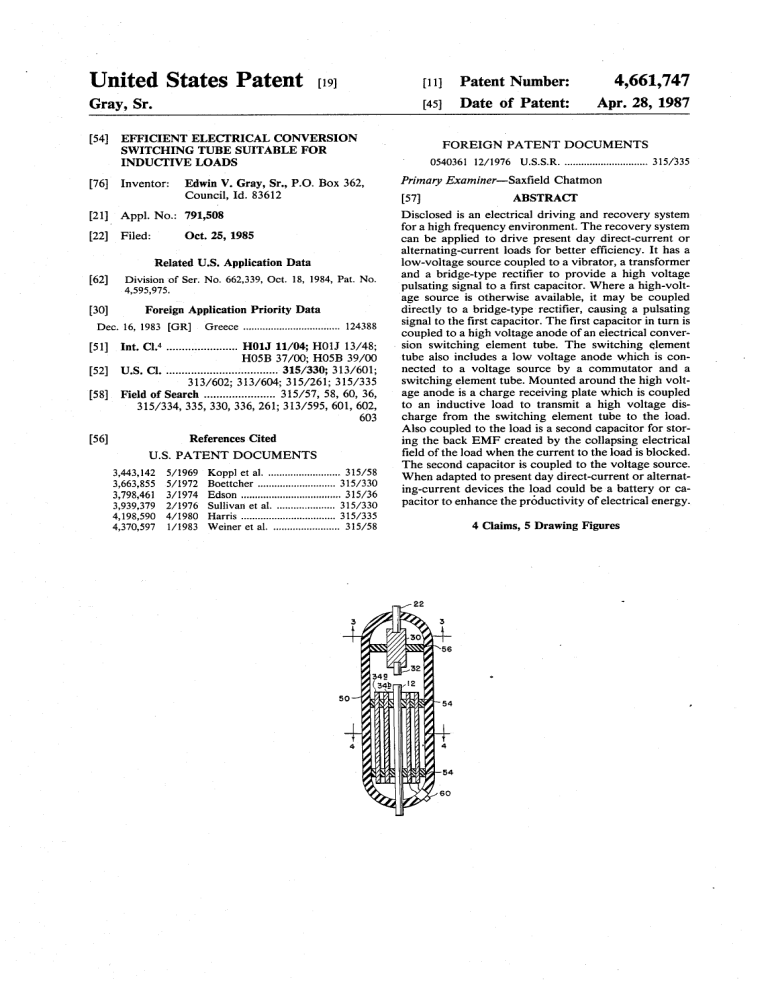
United States Patent (19) Gray, Sr. (54) EFFICIENT ELECTRICAL CONVERSION Council, Id. 83612 21 Appl. No.: 791,508 Oct. 25, 1985 22 Filed: 62) Division of Ser. No. 662,339, Oct. 18, 1984, Pat. No. 4,595,975. Foreign Application Priority Data Dec. 16, 1983 GR) Greece................................... 124388 Int. Cl........................ H01J 11/04; H01J 13/48; H05B 37/00; H05B 39/00 52 U.S. Cl. .................................... 315/330; 313/601; 313/602; 313/604; 315/261; 315/335 58 Field of Search ....................... 315/57, 58, 60, 36, 315/334, 335, 330,336,261; 313/595, 601, 602, 603 References Cited U.S. PATENT DOCUMENTS 3,443,142 3,663,855 3,798,461 3,939,379 5/1969 5/1972 3/1974 2/1976 Koppl et al. .......................... 315/58 Boettcher. ... 315/330 Edson ................................... 35/36 Sullivan et al. ... 315/330 4,198,590 4/1980 Harris................ Primary Examiner-Saxfield Chatmon (57) Related U.S. Application Data (56) Apr. 28, 1987 054036l 12/1976 U.S.S.R. .............................. 315/335 76 Inventor: Edwin V. Gray, Sr., P.O. Box 362, 51 4,661,747 FOREIGN PATENT DOCUMENTS SWITCHINGTUBE SUTABLE FOR INDUCTIVE LOADS 30) Patent Number: Date of Patent: 11 45 ABSTRACT Disclosed is an electrical driving and recovery system for a high frequency environment. The recovery system can be applied to drive present day direct-current or alternating-current loads for better efficiency. It has a low-voltage source coupled to a vibrator, a transformer and a bridge-type rectifier to provide a high voltage pulsating signal to a first capacitor. Where a high-volt age source is otherwise available, it may be coupled directly to a bridge-type rectifier, causing a pulsating signal to the first capacitor. The first capacitor in turn is coupled to a high voltage anode of an electrical conver sion switching element tube. The switching element tube also includes a low voltage anode which is con nected to a voltage source by a commutator and a switching element tube. Mounted around the high volt age anode is a charge receiving plate which is coupled to an inductive load to transmit a high voltage dis charge from the switching element tube to the load. Also coupled to the load is a second capacitor for stor ing the back EMF created by the collapsing electrical field of the load when the current to the load is blocked. The second capacitor is coupled to the voltage source. When adapted to present day direct-current or alternat ing-current devices the load could be a battery or ca pacitor to enhance the productivity of electrical energy. ... 315/335 4 Claims, 5 Drawing Figures 4,370,597 1/1983 Weiner et al. ........................ 315/58 22 2 2 3%MY56 2N 2NWS2 2 3 2 49 2. 2 w 2 50 2: $2 54 %3A% %3A% AAAW 2.3% MAAA% 2. $2 54 2.& 23 EY 60 8 U.S. Patent Apr. 28, 1987 Sheet 1 of 2 4,661,747 F G. U.S. Patent Apr. 28, 1987 li cò CN] S F G. 3 n?) Sheet 2 of 2 4,661,747 1. 4,661,747 2 charge receiving element; conducting the discharge to an inductive load; coupling a second capacitor to the load; and coupling the second capacitor to the source. It is an aim of the present invention to provide a system for driving an inductive load which system is substantially more efficient than any now existing. EFFICIENT ELECTRICAL CONVERSION SWITCHING TUBE SUTABLE FOR INDUCTIVE LOADS This is a division of application Ser. No. 662,339, filed Another object of the present invention is to provide Oct. 18, 1984, now U.S. Pat. No. 4,595,975. BACKGROUND OF THE INVENTION 1. Field of the Invention O a system for driving an inductive load which is reliable, is inexpensive and simply constructed. The foregoing objects of the present invention to gether with various other objects, advantages, features The present invention relates to an electrical driving system and a conversion element, and more particu and results thereof which will be evident to those skilled larly, to a system for driving an inductive load in a in the art in light of this disclosure may be achieved greatly improved and efficient manner. with the exemplary embodiment of the invention de 15 scribed in detail hereinafter and illustrated in the ac 2. Description of the Prior Act In the opinion of the inventor, there is no known companying drawings. device which provides the conversion of energy from a BRIEF DESCRIPTION OF THE DRAWINGS direct-current electric source or an alternating-current electric source to a mechanical force based on the prin FIG. 1 is a schematic circuit diagram of the electrical ciple of this invention. EXAMPLE: A portable energy 20 driving system. FIG. 2 is an elevational sectional view of the electri source, (1) such as a battery, (2) such as alternating-cur rent, (3) such as the combination of battery and alternat cal conversion element. ing-current, may be used with highly improved effi FIG. 3 is a plan sectional view taken along line 3-3 ciency to operate a mechanical device, whose output is of FIG. 2. a linear or rotary force, with an attendant increase in the 25 FIG. 4 is a plan sectional view taken along line 4-4 useful productive period between external applications of FIG. 2. of energy restoration for the energy source. FIG. 5 is a schematic circuit diagram of the alternat ing-current input circuit. SUMMARY OF THE INVENTION The present invention provides a more efficient driv ing system comprising a source of electrical voltage; a vibrator connected to the low-voltage source for form ing a pulsating signal; a transformer connected to the vibrator for receiving the pulsating signal; a high-volt age source, where available, connected to a bridge-type rectifier; or the bridge-type rectifier connected to the high voltage pulse output of the transformer; a capaci tor for receiving the voltage pulse output; a conversion element having first and second anodes, electrically conductive means for receiving a charge positioned about the second anode and an output terminal con nected to the charge receiving means, the second anode being connected to the capacitor; a commutator con nected to the source of electrical voltage and to the first anode; and an inductive load connected to the output terminal whereby a high energy discharge between the first and second anodes is transferred to the charge receiving means and then to the inductive load. As a sub-combination, the present invention also in cludes a conversion element comprising a housing; a first low voltage anode mounted to the housing, the first 30 While the present invention is susceptible of various modifications and alternative constructions, an embodi ment is shown in the drawings and will herein be de 35 scribed in detail. It should be understood however that it is not the intention to limit the invention to the partic ular form disclosed; but, on the contrary, the invention is to cover all modifications, equivalents and alternative 45 50 anode adapted to be connected to a voltage source; a second high voltage anode mounted to the housing, the second anode adapted to be connected to a voltage source; electrically conductive means positioned about the second anode and spaced therefrom for receiving a charge, the charge receiving means being mounted to the housing; and an output terminal communicating with the charge receiving means, said terminal adapted to be connected to an inductive load. DESCRIPTION OF THE PREFERRED EMBODIMENT 55 60 The invention also includes a method for providing power to an inductive load comprising the steps of providing a voltage source, pulsating a signal from said source; increasing the voltage of said signal; rectifying said signal; storing and increasing the signal; conducting 65 said signal to a high voltage anode; providing a low voltage to a second anode to form a high energy dis charge; electrostatically coupling the discharge to a constructions falling within the spirit and scope of the invention as expressed in the appended claims. There is disclosed herein an electrical driving system which, on theory, will convert low voltage electric energy from a source such as an electric storage battery to a high potential, high current energy pulse that is capable of developing a working force at the inductive output of the device that is more efficient than that which is capable of being developed directly from the energy source. The improvement in efficiency is further enhanced by the capability of the device to return that portion of the initial energy developed, and not used by the inductive load in the production of mechanical en ergy, to the same or second energy reservoir or source for use elsewhere, or for storage. This system accomplishes the results stated above by harnessing the "electrostatic' or "impulse' energy cre ated by a high-intensity spark generated within a spe cially constructed electrical conversion switching ele ment tube. This element utilizes a low-voltage anode, a high-voltage anode, and one or more "electrostatic' or charge receiving grids. These grids are of a physical size, and appropriately positioned, as to be compatible with the size of the tube, and therefore, directly related to the amount of energy to be anticipated when the device is operating. The low-voltage anode may incorporate a resistive device to aid in controlling the amount of current drawn from the energy source. This low-voltage anode is connected to the energy source through a mechanical 4,661,747 4 A novel, but not essential, circuit arrangement pro 3 commutator or a solid-state pulser that controls the vides for switching the energy source and the energy timing and duration of the energy spark within the storage device. This switching may be so arranged as to actuate automatically at predetermined times. The switching may be at specified periods determined by experimentation with a particular device, or may be actuated by some control device that measures the rela element. The high-voltage anode is connected to a high voltage potential developed by the associated circuits. An energy discharge occurs within the element when the external control circuits permit. This short duration, high-voltage, high-current energy pulse is captured by the "electrostatic' grids within the tube, stored momen tarily, then transferred to the inductive output load. The increase in efficiency anticipated in converting tive energy content of the two energy reservoirs. Referring now to FIG. 1, the system 10 will be de 10 inductive load is attributed to the utilization of the most optimum timing in introducing the electrical energy to the load device, for the optimum period of time. Further enhancement of energy conservation is ac complished by capturing a significant portion of the energy generated by the inductive load when the useful energy field is collapsing. This energy is normally dissi pated in load losses that are contrary to the desired energy utilization, and have heretofore been accepted because no suitable means had been developed to har ness this energy and restore it to a suitable energy stor age device. The present invention is concerned with two con cepts or characteristics. The first of these characteristics is observed with the introduction of an energizing cur rent through the inductor. The inductor creates a con 5 25 trary force (counter-electromotive force or CEMF) that opposes the energy introduced into the inductor. This CEMF increases throughout the time the intro duced energy is increasing. In normal applications of an alternating-current to an inductive load for mechanical applications, the useful work of the inductor is accomplished prior to terminat ing the application of energy. The excess energy applied 30 35 is thereby wasted. Previous attempts to provide energy inputs to an inductor of time durations limited to that period when the optimum transfer of inductive energy to mechanical energy is occuring, have been limited by the ability of 40 The second characteristic is observed when the ener previously been lost due to a failure to provide a storage capability for this energy. In this invention, a high-voltage, high-current, short duration energy pulse is applied to the inductive load by the conversion element. This element makes possible the use of certain of that energy impressed within an arc across a spark-gap, without the resultant deterioration of circuit elements normally associated with high en ergy electrical arcs. This invention also provides for capture of a certain portion of the energy induced by the high inductive kick produced by the abrupt withdrawal of the intro duced current. This abrupt withdrawal of current is attendant upon the termination of the stimulating arc. The voltage spike so created is imposed upon a capaci tor that couples the attendant current to a secondary energy storage device. oped across the capacitor 16. This voltage is produced by drawing a low current from a battery source 18 through the vibrator 20. The effect of the vibrator is to create a pulsating input to the transformer 22. The turns ratio of the transformer is chosen to optimize the volt age applied to a bridge-type rectifier 24. The output of the rectifier is then a series of high-voltage pulses of modest current. When the available source is already of the high voltage AC type, it may be coupled directly to the bridge-type rectifier. By repetitious application of these output pulses from the bridge-type recrifier to the capacitor 16, a high-volt age high-level charge is built up on the capacitor. Control of the conversion switching element tube is maintained by a commutator 26. A series of contacts mounted radially about a shaft, or a solid-state switch ing device sensitive to time or other variable may be used for this control element. A switching element tube type one-way energy path 28 is introduced between the commutator device and the conversion switching ele ment tube to prevent high energy arcing at the commu tator current path. When the switching element tube is closed, current from the voltage source 18 is routed through a resistive element 30 and a low voltage anode 32. This causes a high energy discharge between the anodes within the conversion switching element tube 14. any such device to handle the high current required to optimize the energy transfer. gizing current is removed from the inductor. As the current is decreased, the inductor generates an EMF that opposes the removal of current or, in other words, produces an energy source at the output of the inductor that simulates the original energy source, reduced by the actual energy removed from the circuit by the me chanical load. This "regenerated', or excess, energy has scribed in additional detail. The potential for the high voltage anode 12 of the conversion element 14 is devel the electrical energy to mechanical energy within the 45 50 The energy content of the high energy pulse is elec trostatically coupled to the conversion grids 34 of the conversion element. This electrostatic charge is applied through an output terminal 60 (FIG. 2) across the load inductance 36, inducing a strong electromagnetic field about the inductive load. The intensity of this electro magnetic field is determined by the high electromotive potential developed upon the electrostatic grids and the very short time duration required to develop the energy pulse. If the inductive load is coupled magnetically to a mechanical load, a strong initial torque is developed that may be efficiently utilized to produce physical work. 55 Upon cessation of the energy pulse (arc) within the conversion switching element tube the inductive load is decoupled, allowing the electromagnetic field about the inductive load to collapse. The collapse of this energy field induces within the inductive load a counter EMF. 60 65 This counter EMF creates a high positive potential across a second capacitor 38 which, in turn, is induced into the second energy storage device or battery 40 as a charging current. The amount of charging current available to the battery 40 is dependent upon the initial conditions within the circuit at the time of discharge within the conversion switching element tube and the amount of mechanical energy consumed by the work load. A spark-gap protection device 42 is included in the circuit to protect the inductive load and the rectifier 4,661,747 6 stored on the capacitor in incremental, additive steps the potentials within the circuit exceed predetermined from the bridge-type rectifier 24. When the energy source is a direct-current electric values, fixed by the mechanical size and spacing of the elements within the protective device, the excess en energy storage device, such as the battery 12, the input ergy is dissipated (bypassed) by the protective device to 5 to the bridge rectifier is provided by the voltage step-up transformer 22, that is in turn energized from the vibra the circuit common (electrical ground). Diodes 44 and 46 bypass the excess overshoot gener tor 20, or solid-state chopper, or similar device to prop ated when the "Energy Conversion Switching Element erly drive the transformer and rectifier circuits. Tube' is triggered. A switching element 48 allows ei O When the energy source is an alternating-current, ther energy storage source to be used as the primary switches 64 disconnect transformer 22 and the input to energy source, while the other battery is used as the the bridge-type rectifier 24 is provided by the voltage energy retrieval unit. The switch facilitates interchang step-up transformer 66, that is in turn energized from ing the source and the retrieval unit at optimum inter the vibrator 20, or solid-state chopper, or similar device vals to be determined by the utilization of the conver to properly drive the transformer and rectifier circuits. sion switching element tube. This switching may be 15 The repetitious output of the bridge rectifier incre increases the capacitor charge toward its max accomplished manually or automatically, as determined mentally imum. This charge is electrically connected directly to by the choice of switching element from among a large the high-voltage anode 12 of the conversion switching variety readily available for the purpose. FIGS. 2, 3, and 4 show the mechanical structure of element tube. When the low-voltage anode 32 is connected to a the conversion switching element tube 14. An outer 20 source of current, an arc is created in the spark-gap housing 50 may be of any insulative material such as designated of the conversion switching element tube glass. The anodes 12 and 32 and grids 34a and 34b are equivalent 62 to potential stored on the high-voltage firmly secured by nonconductive spacer material 54, anode, and thethecurrent available from the low-voltage and 56. The resistive element 30 may be introduced into 25 anode. Because the duration of the arc is very short, the the low-voltage anode path to control the peak currents instantaneous voltage, and instantaneous current may through the conversion switching element tube. The both be very high. The instantaneous peak resistive element may be of a piece, or it may be built of power is therefore, also very high. Within theapparent conver one or more resistive elements to achieve the desired sion switching element tube, this energy is absorbed by result. 30 the grids 34a and 34b mounted circumferentially about The anode material may be identical for each anode, the interior of the tube. or may be of differing materials for each anode, as dic Control of the energy spike within the conversion tated by the most efficient utilization of the device, as switching element tube is accomplished by a mechani determined by appropriate research at the time of pro cal, or solid-state commutator, that closes the circuit duction for the intended use. 35 path from the low-voltage anode to the current source The shape and spacing of the electrostatic grids is at that moment when the delivery of energy to the also susceptible to variation with application (voltage, output load is most auspicious. Any number of standard current, and energy requirements). high-accuracy, variable setting devices are available for It is the contention of the inventor that by judicious this purpose. When control of the repetitive rate of the mating of the elements of the conversion switching 40 system's output is required, it is accomplished by con element tube, and the proper selection of the compo trolling the time of connection at the low-voltage an nents of the circuit elements of the system, the desired ode. theoretical results may be achieved. It is the inventor's Thus there can be provided an electrical driving contention that this mating and selection process is well system having a low-voltage source coupled to a vibra within the capabilities of intensive research and devel 45 tor, a transformer and a bridge-type rectifier to provide opment technique. a high voltage pulsating signal to a first capacitor. Let it be stated here that substituting a source of Where a high-voltage source is otherwise available, it electric alternating-current subject to the required cur may be coupled direct to a bridge-type rectifier, causing rent and/or voltage shaping and/or timing, either prior a pulsating signal to a first capacitor. The capacitor in to being considered a primary energy source, or there 50 turn is coupled to a high-voltage anode of an electrical after, should not be construed to change the described conversion switching element tube. The element also utilization or application of primary energy in any way. includes a low-voltage anode which in turn is con Such energy conversion is readily achieved by any of a nected to a voltage source by a commutator, a switch multitude of well established principles. The preferred ing element tube, and a variable resistor. Mounted embodiment of this invention merely assumes optimum 55 around the high-voltage anode is a charge receiving utilization and optimum benefit from this invention plate which in turn is coupled to an inductive load to when used with portable energy devices similar in prin transmit a high-voltage discharge from the element to ciple to the wet-cell or dry-cell battery. the load. Also coupled to the load is a second capacitor This invention proposes to utilize the energy con for storing the back EMF created by the collapsing tained in an internally generated high-voltage electric 60 electrical field of the load when the current to the load spike (energy pulse) to electrically energize an induc is blocked. The second capacitor in turn is coupled to tive load; this inductive load being then capable of con the voltage source. What is claimed is: verting the energy so supplied into a useful electrical or 1. An electrical conversion switching element tube mechanical output In operation the high-voltage, short-duration electric 65 comprising: 5 elements from unduly large discharge currents. Should spike is generated by discharging the capacitor 16 across the spark-gap in the conversion switching ele ment tube. The necessary high-voltage potential is a closed insulative housing (50); a first low-voltage anode (32) mounted internally to said housing and extending internally to an electri 7 4,661,747 cal discharge area (62), said first anode adapted to be connected to a voltage source external to the housing; a second high-voltage anode (12) mounted internally to said housing and extending internally to said electrical discharge area (62), said second anode also being adapted to be connected to a voltage source external to the housing: electrically conductive means (34b) positioned inter nally within said housing and extending circumfer entially about said second anode while being di rectly exposed thereto but not conductively con nected thereto but, rather, spaced therefrom for receiving an electrostatic charge from the second anode when a discharge current is triggered across said discharge area between said first and second anodes, said charge receiving electrically conduc 5 8 tive means also being internally mounted to said housing; and an output terminal (60) communicating with said charge receiving electrically conductive means, said terminal adapted to be connected to an induc tive load externally of said housing. 2. An electrical conversion switching element tube as claimed in claim 1, including a resistive element (30) in series with said first anode. 10 3. An electrical conversion switching element tube as said charge receiving electrically conductive means is claimed in claim 1 wherein: 5 tubularly shaped. 4. An electrical conversion switching element tube as claimed in claim 3, including a second tubularly shaped charge receiving electri cally conductive means (34a) positioned circumfer entially about said first mentioned charge receiving electrically conductive means. k 25 30 35 45 50 55 60 65
